Graphene has spent years wearing the crown of “future miracle material,” which is a dangerous title because it tends to attract both Nobel-level science and wildly optimistic PowerPoint decks. Stronger than steel, thinner than a rumor, and able to move electrons with remarkable speed, graphene sounds like the material that should have taken over electronics by now. Yet for chipmakers, the question has never been simply, “Is graphene amazing?” It has been, “Can we manufacture it reliably, at scale, on wafers, without turning the fab into a science fair volcano?”
That is why the idea of graphene grown directly on semiconductors matters so much. The breakthrough associated with growing graphene nanoribbons on germanium was not just another laboratory curiosity. It addressed one of the most stubborn barriers in graphene electronics: how to make useful, narrow, well-oriented graphene structures on a substrate that already speaks the language of semiconductor manufacturing.
In other words, this is not only a story about a wonder material. It is a story about manufacturability, repeatability, and whether graphene can move from “cool under a microscope” to “useful on a wafer.” For a material with a résumé this flashy, learning to behave in a factory may be its greatest achievement.
Why Graphene Still Makes Engineers Lean Forward
Graphene is a single layer of carbon atoms arranged in a honeycomb lattice. That simple description hides an absurd collection of properties. It is atomically thin, mechanically strong, flexible, thermally conductive, and electrically impressive. Electrons can move through high-quality graphene with exceptional mobility, which is why researchers have long imagined graphene transistors, sensors, radio-frequency devices, photodetectors, and hybrid integrated circuits.
The promise is especially tempting in electronics. Traditional silicon technology has been refined for decades, but shrinking devices further becomes harder, hotter, and more expensive. Graphene offers a tantalizing alternative because it can carry charge quickly and survive at dimensions where ordinary materials start wheezing like an old laptop fan.
However, graphene has a personality flaw. In its natural form, it behaves like a semimetal rather than a conventional semiconductor. Digital logic needs a material that can switch cleanly between “on” and “off.” Pristine graphene is excellent at conducting, but it is not naturally excellent at stopping. That is a bit like hiring a racehorse to work as a traffic light.
The Band Gap Problem: Graphene’s Great Awkward Dinner Guest
For graphene to become useful in many transistor applications, engineers need a band gap. A band gap allows a semiconductor device to switch current off with enough control for logic circuits. Without it, graphene transistors can be fast but leaky, and leaky logic is not the foundation of a happy computer.
One way to create a band gap is to cut graphene into extremely narrow strips called graphene nanoribbons. When graphene is confined into ribbons just a few nanometers wide, quantum effects and edge structure can change its electronic behavior. The result can be semiconducting graphene, especially when the ribbon edges are smooth and arranged in the desired “armchair” orientation.
That sounds simple until you try to make it. Cutting graphene into nanoribbons with rough edges can destroy the very properties that made graphene exciting in the first place. Top-down patterning methods may work for demonstrations, but atomically rough edges are bad news for electronics. A graphene nanoribbon is only as good as its edges, and at this scale, “close enough” is the villain wearing a lab coat.
What Made Growing Graphene On Germanium So Important?
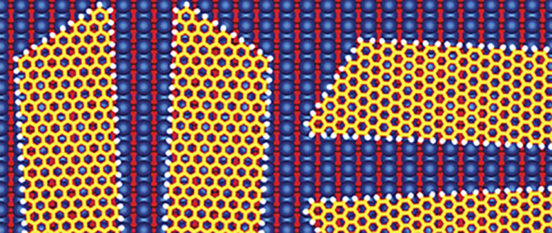
The major step forward came from growing graphene nanoribbons directly on germanium, a semiconductor material with a long history in electronics. Researchers used chemical vapor deposition, or CVD, a familiar manufacturing-related process in which gases react at a surface to form a material. In this case, methane served as a carbon source, and the germanium crystal helped guide the growth.
The remarkable part was directionality. On the germanium surface, graphene did not simply spread randomly like spilled coffee. It formed narrow ribbons that aligned along specific crystal directions. Even better, those ribbons could have smooth armchair edges, the kind of edge structure needed for semiconducting behavior.
That is a big deal because semiconductor manufacturing is built around control. A chip fab does not want a material that grows wherever it feels inspired. It wants repeatable placement, predictable orientation, compatible substrates, and process steps that can eventually be scaled. Growing graphene nanoribbons directly on germanium brings the material closer to that world.
Why Germanium Is More Than A Historical Footnote
Germanium is not some random slab chosen because it happened to be nearby. It was used in the earliest transistors and remains relevant in advanced semiconductor research. Importantly, germanium can be integrated with silicon-based platforms and can be prepared as a crystalline semiconductor surface.
For graphene nanoribbons, germanium offers a useful template. Its crystal surface can encourage anisotropic growth, meaning growth is faster in one direction than another. This helps form long, narrow structures rather than broad, irregular patches. The substrate is not just a table where graphene sits; it is more like a dance floor with arrows painted on it.
Bottom-Up Growth Beats Atomic-Scale Whittling
There are two broad ways to make tiny structures: carve them out or grow them into shape. Carving, or top-down fabrication, dominates modern chipmaking, but graphene nanoribbons are so small and edge-sensitive that carving can leave damage. A rough edge at the atomic scale can ruin electronic behavior.
Bottom-up growth offers a more elegant route. Instead of cutting a large sheet into tiny ribbons, researchers encourage the ribbons to form directly with the desired structure. The germanium-based approach is exciting because it uses the substrate itself to guide that growth. The material begins to assemble in a useful shape rather than being forced into one after the fact.
Later research on molecular seeds and controlled nanoribbon growth continued this theme. By starting growth from carefully chosen carbon-based molecules, scientists have explored ways to control where ribbons begin, how narrow they become, and how consistently they extend. This is the kind of progress that matters for real electronics, because factories prefer recipes over miracles.
Why Manufacturability Is The Real Headline
In materials science, a discovery can be scientifically brilliant and commercially useless at the same time. The graveyard of “next big things” is full of materials that worked beautifully once, on a sample the size of a breadcrumb, when handled by a patient graduate student after three coffees and a pep talk.
Manufacturability asks tougher questions. Can the material be grown across a wafer? Can it be patterned? Can it be measured? Can the process survive contamination controls, thermal budgets, etching, contacts, dielectrics, packaging, and quality control? Can different devices on the same wafer perform similarly? Can the process run again next Tuesday and produce the same result?
Graphene grown directly on semiconductors matters because it reduces some of the mess associated with transferring graphene from one surface to another. Transfer steps can introduce wrinkles, tears, residues, cracks, and alignment problems. For a consumer device, those are defects. For a chip fab, those are tiny career-ending gremlins.
Direct growth on a semiconductor platform suggests a cleaner path. It does not solve every problem, but it moves graphene closer to the toolsets, substrates, and workflows used by the semiconductor industry. That is why “grown on semiconductors” is not a boring technical detail. It is the bridge between material promise and manufacturing reality.
How This Fits Into The Bigger Graphene Semiconductor Race
The germanium nanoribbon work is part of a larger push to make graphene useful in electronics. Epitaxial graphene on silicon carbide has produced high-frequency transistor demonstrations. More recently, semiconducting epigraphene on silicon carbide has shown a real band gap and high mobility, renewing excitement about graphene-based semiconductor platforms.
Meanwhile, wafer-scale graphene research has moved from isolated lab devices toward pilot lines, multi-project wafer runs, and process optimization. That shift is crucial. The semiconductor industry does not adopt a material because it wins a beauty contest under Raman spectroscopy. It adopts a material when engineers can measure yield, variability, contact resistance, mobility, hysteresis, contamination, and failure modes across many devices.
Graphene may first succeed in specialized applications rather than replacing silicon logic overnight. Radio-frequency electronics, sensors, photonics, flexible electronics, biosensing, quantum devices, interconnects, and hybrid circuits may all offer more realistic entry points. Silicon is not being evicted tomorrow. It owns the building, knows the landlord, and has decades of process integration behind it.
Potential Applications: Where Graphene Nanoribbons Could Shine
Faster, Lower-Power Transistors
If graphene nanoribbons can be grown with consistent width, orientation, and edge structure, they could support transistor channels with high mobility and useful switching behavior. That combination is the dream: fast charge transport plus a controllable off state. The challenge is making billions of those channels behave politely at the same time.
Hybrid Integrated Circuits
Graphene does not need to overthrow silicon to be valuable. It could be integrated into hybrid circuits where silicon handles mature logic and graphene handles specialized functions. Think of graphene as the fast, exotic specialist brought in for tasks that silicon finds annoying.
High-Frequency And RF Devices
Graphene’s high carrier mobility makes it attractive for radio-frequency and high-speed electronics. Even where it is not ideal for digital logic, it may perform well in analog, RF, and communication-related devices. In these applications, speed and signal handling can matter more than perfect digital switching.
Sensors And Detectors
Because graphene is atomically thin, its entire surface is exposed to the environment. That makes it highly sensitive to chemical, biological, and electrical changes. Directly grown graphene structures on semiconductor wafers could enable compact sensors that are easier to integrate with readout electronics.
The Challenges Still Standing In The Way
The road to graphene manufacturability is still paved with difficult engineering. First, uniformity matters. A ribbon that is five nanometers wide in one region and eight nanometers wide in another may not behave the same way. At this scale, tiny differences are not tiny.
Second, contacts are a headache. A great channel material can be wasted if the metal contacts inject charge poorly. Contact resistance has haunted many next-generation transistor materials, and graphene is no exception.
Third, integration with dielectrics and gates must be solved without damaging the graphene. Atomically thin materials are sensitive. They are not fond of rough processing, aggressive chemicals, or being treated like a chunk of bulk silicon.
Fourth, the process must scale. A beautiful result on a small crystal is an achievement. A repeatable process across large wafers is a technology. The distance between those two is where many graduate theses go to become footnotes.
Why This Breakthrough Still Matters Years Later
The original graphene-on-germanium result remains important because it pointed toward a practical philosophy: do not merely make graphene; make graphene where electronics already live. Growing graphene nanoribbons on a semiconductor substrate reframed the problem from material discovery to process integration.
That mindset continues to shape current research. Modern work on semiconducting epigraphene, wafer-scale graphene films, 2D material pilot lines, and controlled nanoribbon synthesis all follows the same basic logic. The future of graphene electronics depends less on hype and more on boring, beautiful manufacturing details.
And that is the funny part. Graphene became famous because it sounded futuristic. Its path to usefulness may depend on becoming ordinary enough for a factory. The miracle material has to learn shift work.
Experience-Based Perspective: What This Topic Teaches About Real Innovation
When looking at a topic like graphene grown on semiconductors, one of the most useful experiences is learning to separate scientific excitement from manufacturing readiness. In technology writing, it is tempting to treat every lab result as if a new phone, laptop, or quantum toaster will arrive by Christmas. But semiconductor progress is rarely that dramatic. It is usually a long march of process control, measurement, redesign, and stubborn iteration.
The germanium nanoribbon breakthrough is a good example of how real innovation often looks modest from a distance. Nobody walked out of the lab holding a graphene processor ready to challenge Intel, AMD, Apple, or NVIDIA. Instead, researchers showed that graphene could be grown in a more controlled way on a semiconductor surface. That may sound narrow, but in chipmaking, narrow wins. A tiny improvement in alignment, contamination control, or edge smoothness can matter more than a dramatic claim.
Anyone who has followed hardware development knows that compatibility is king. A material can be spectacular, but if it demands entirely new factories, exotic handling, impossible temperatures, or fragile transfer steps, adoption becomes difficult. Semiconductor fabs are among the most expensive and carefully tuned manufacturing environments on Earth. They do not casually invite new materials inside. A new material has to justify itself, behave itself, and preferably avoid shedding defects all over the cleanroom like a carbon-based golden retriever.
That is why direct growth is so compelling. In practical terms, every transfer step is a risk. If graphene is grown somewhere else and then moved, the process can introduce wrinkles, polymer residues, cracks, bubbles, and alignment issues. Those defects may be manageable in research samples, but they become serious problems when thousands or millions of devices must perform consistently. Growing graphene directly on a semiconductor substrate removes at least part of that risk and makes the process feel more like chip manufacturing and less like nanoscale arts and crafts.
Another lesson is that the substrate is not passive. People often imagine a wafer as a flat stage, but at the atomic level, the surface chemistry and crystal orientation can shape what grows on it. Germanium helped guide the graphene into ribbons with a preferred direction. That is a powerful idea. Instead of fighting randomness after growth, engineers can design the growth environment so the material organizes itself more usefully from the beginning.
For readers interested in future electronics, the most realistic takeaway is patience with enthusiasm. Graphene may not replace silicon in mainstream processors soon, and it does not need to do so to be important. Many transformative materials enter through side doors: sensors, RF components, photonics, specialized accelerators, quantum devices, or hybrid systems. Once manufacturing knowledge improves, broader use becomes more believable.
The story also shows why interdisciplinary teams matter. This field sits at the intersection of surface science, materials engineering, chemistry, device physics, and semiconductor processing. No single discipline owns the problem. The people who understand carbon chemistry need the people who understand wafers, and the people who understand wafers need the people who can measure atomic edges without blinking.
In the end, graphene grown on semiconductors is not just a headline about a material. It is a reminder that manufacturability is where big ideas either become technology or remain trivia. Graphene already proved it could amaze scientists. The harder and more valuable task is proving it can behave predictably enough for manufacturing. That is less glamorous than a miracle, but far more useful.
Conclusion
Graphene grown on semiconductors represents a meaningful step toward practical graphene electronics because it tackles the problem that matters most: manufacturability. The ability to grow graphene nanoribbons directly on germanium showed that substrate-guided, bottom-up synthesis could produce narrow, oriented structures with the kind of edge control needed for semiconducting behavior.
The breakthrough does not mean graphene chips are ready to replace silicon tomorrow. It means researchers have found a more realistic path toward integrating graphene with semiconductor manufacturing. Combined with advances in epigraphene, wafer-scale graphene devices, and improved process control, this work helps move graphene from the land of breathless promises toward the more useful world of repeatable engineering.
Graphene’s future will not be decided by hype. It will be decided by wafers, defects, contacts, yields, and whether factories can make the same excellent material again and again. That may sound less magical, but in electronics, repeatability is the real superpower.